Installation practice and modular grounding features
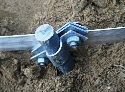 Modular grounding is a project created specifically for the installation of grounding conductors in residential facilities, for example, such as suburban private houses, country houses, as well as for industrial and administrative facilities.
The modular earthing switch is a prefabricated structure consisting of steel pins specially treated with copper, each 1.5 meters long. These pins are combined into a single grounding ground loop of the object.
The length of the prefabricated grounding pin can reach a depth of about 30 - 40 meters. Earthing 1.5 meter pins have threads at the ends, through which the couplings between them, it becomes possible as the precast earthing pin moves in depth - to increase it with the next pin, etc. The installation of the vertical grounding pin in depth is done as follows ...
Highlights of using safe voltage in everyday life
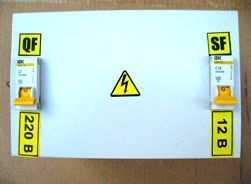 The risk of injuries to humans from electric shocks, both in production and in everyday life, is very high. It is a direct result of non-compliance with safety measures, as well as failure or malfunction of electrical equipment and household appliances. Therefore, the use of safe voltage for our domestic needs is difficult to overestimate. In today's article, we will consider the practice and the main possibilities of using tension safe for humans in our house, cottage or apartment.
What is an electrical voltage safe for humans? Now it is considered safe for humans to have a voltage of 42 Volts (until recently it was 36 V), used for portable lighting and household appliances in the air and in the house and 12 Volts, subject to the use of portable lighting fixtures and appliances inside boilers ...
Transistor operation in key mode
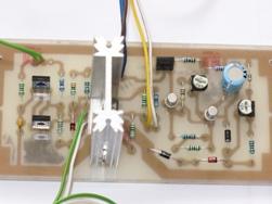 To simplify the story, you can imagine a transistor in the form of a variable resistor. The conclusion of the base is just the very handle that you can twist. In this case, the resistance of the collector - emitter section changes. Of course, you don’t need to twist the base, it can come off. But to apply some voltage to it relative to the emitter, of course, is possible.
If the voltage is not applied at all, but simply take and close the conclusions of the base and emitter, even if not short, but through a resistor of several KOhms. It turns out that the base-emitter voltage (Ube) is zero. Consequently, there is no base current. The transistor is closed, the collector current is negligible, just the same initial current. About the same as a diode in the opposite direction! In this case, they say that the transistor is in the OFF position, which in ordinary language means it is closed or locked. The opposite state is called saturation ...
Characteristics of Bipolar Transistors
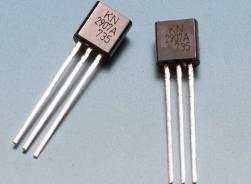 At the very end of the previous part of the article, a “discovery” was made. Its meaning is that a small base current controls a large collector current. This is precisely the main property of the transistor, its ability to amplify electrical signals. In order to continue the further narration, it is necessary to understand how large the difference of these currents is, and how this control occurs.
To better remember what is being said, the figure shows an n-p-n transistor with power supplies for the base and collector circuits connected to it. Everything that is told about the transistor of the n-p-n structure is quite true for the p-n-p transistor. Only in this case should the polarity of the power sources be reversed. And in the description itself, “electrons” should be replaced with “holes”, wherever they occur. But at present, transistors of the n-p-n structure are more modern, more in demand ...
The device and operation of the bipolar transistor
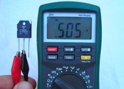 A transistor is an active semiconductor device, with the help of which amplification, conversion and generation of electrical oscillations is carried out. Such an application of the transistor can be observed in analogue technology. In addition, transistors are also used in digital technology, where they are used in key mode. But in digital equipment, almost all transistors are “hidden” inside integrated circuits, and in huge quantities and in microscopic dimensions.
Here we will not dwell too much on the electrons, holes and atoms, which were already described in the previous parts of the article, but some of this, if necessary, will still have to be remembered. The transistor consists of two transitions, so the diode can be considered as the precursor of the transistor, or its half. If the p-n junction is at rest ...
Characteristics of diodes, designs and application features
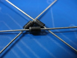 In a previous article, we started introducing a semiconductor diode. In this article we will consider the properties of diodes, their advantages and disadvantages, various designs and features of application in electronic circuits.
The current-voltage characteristic (CVC) of a semiconductor diode is shown in the figure. Here, in one figure, the I – V characteristics of germanium (blue) and silicon (black) diodes are shown. It is easy to notice that the characteristics are very similar. There are no numbers on the coordinate axes, since for different types of diodes they can vary significantly: a powerful diode can pass a direct current of several tens of amperes, while a low-power one can only transmit several tens or hundreds of milliamps. There are a great many diodes of different models, and they all can have different purposes, although their main task, the main property is ...
How semiconductor diodes are arranged and work
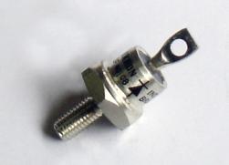 Diodine - the simplest device in the glorious family of semiconductor devices. If we take a plate of a semiconductor, for example Germany, and introduce an acceptor impurity into its left half, and into the donor right, then on the one hand we get a type P semiconductor, respectively, on the other type N. In the middle of the crystal we get the so-called P-N junction.
The figure below shows the conventional graphic designation of the diode in the diagrams: the cathode output (negative electrode) is very similar to the “-" sign. It’s easier to remember. In total, in such a crystal there are two zones with different conductivities, from which two leads emerge, therefore the resulting device was called a diode, since the prefix "di" means two. In this case, the diode turned out to be a semiconductor, but similar devices were known before: for example, in the era of electron tubes there was a tube diode called a kenotron ...
Transistors Part 3. What transistors are made of
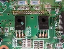 Pure semiconductors have the same amount of free electrons and holes. Such semiconductors are not used for the manufacture of semiconductor devices, as was mentioned in the previous part of the article.
For the production of transistors (in this case, they also mean diodes, microcircuits, and actually all semiconductor devices), n and p types of semiconductors are used: with electronic and hole conductivity. In n-type semiconductors, electrons are the main charge carriers, and holes in p-type semiconductors.
Semiconductors with the required type of conductivity are obtained by doping (adding impurities) to pure semiconductors. The amount of these impurities is small, but the properties of the semiconductor change beyond recognition. Transistors would not be transistors if they were not used in their production ...
